Interface Fermi-Level Engineering: An Innovative Approach to Doping Challenges
Achieving effective p-type doping remains a major challenge in CdTe, nitrides, and various oxides. The high dopant activation energies in these materials limit the concentration of ionized carriers, thereby impeding device performance.
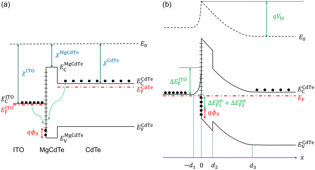
To address this issue, we have developed an innovative approach—interface Fermi-level engineering—using interface states and charge transfer effects to tailor Fermi level without the use of any p-type materials in CdTe solar cells. The devices were fabricated using high-quality monocrystalline CdTe/MgCdTe DH grown by molecular beam epitaxy and a transparent conductive ITO layer was sputtered on top to serve as the front contact.This design produces a strong built-in electric field and achieves open-circuit voltages exceeding 1 V.
Our collaborators, Professor Jack Ma’s team at University of Wisconsin–Madison have confirmed the Fermi-level engineering at the ITO/(Mg)CdTe interface using X-ray photoelectron spectroscopy (XPS) measurements. And the US National Renewable Energy Laboratory (NREL) has confirmed a Voc exceeding 1 V and efficient carrier collection of the device, demonstrating the effectiveness of the all-n-type design. All the results of this study have been published in Solar RRL (link).
This work also caught the attention of Compound Semiconductor, which featured it in a recent article (link). The article highlights how this approach could change the way future optoelectronic and solar devices are designed since the same Fermi-level engineering approach can be readily extended to other semiconductors with doping issues, such as III-nitrides, oxides, diamond, HgCdTe etc.
We welcome all interested researchers and industry partners to read the full article and reach out to us for further discussion or collaboration on this technology.